LABORATORY OF BIO-MECHATRONICS AND MICRO / NANO ENGINEERING FOR MECHATRONIC TECHNOLOGIES, ELEMENTS AND SYSTEMS
SECTION FOR MICRO/NANOASSEMBLING AND MICROPACKAING
PROJECT BG05M2OP001-1.001-0008 | NATIONAL CENTER OF MECHATRONICS AND CLEAN TECHNOLOGIES
Manager: Prof. Valentin Videkov, PhD, Technical University of Sofia, Faculty of Electronic Engineering and Technologies
contacts:
e-mail: videkov@tu-sofia.bg
phone: +359 882 270 558
In this section mounting of semiconductor crystals and packaged microchips is conducted for micromodules with application in the mechatronics and other systems. For this purpose, studies of various coatings and nanomaterials on flexible, solid-state and three-dimensional substrates are carried out in order to improve the possibilities for mounting by using adhesives, solders, pastes, ultrasonic and other methods.
ACTIVITIES
The activity of the section is focused on assembly and micropackaging of microelements (semiconductor crystals, MEMS structures, chip sensors, etc.) in micromodules. The main problems that can be solved are:
- Placing microelements on rigid and flexible planar substrates using adhesives
- Soldering crystals on various metallized substrates by conductive soldering with high precision;
- Microelements soldering in inert atmosphere;
- Ultrasonic welding to metalized surfaces;
- Bonding by gold or aluminum wire on the contact leads of microelements and substrates by butt welding, or side welding;
- Metallizing of variety of substrates for the needs of the mounting and assembling;
- Placing elements by the technology of inverted mounting;
- Strength testing of welded conductors to determine the optimal welding modes to different surfaces;
- Development of processes with diffusive soldering;
- Application of nanomaterials and elements in the mounting process.
SERVICES
In preparation of performing:
- Prototype assembly with high precision (1µm) on substrates with dimensions up to 100x200 mm.
- Joint of microcrystals by conductive soldering with solders at temperatures up to 400° С:
- Ultrasonic welding of crystals;
- Gluing with adhesives through a dispenser;
- Soldering by high speed heating up to 30 °С/s;
- Bonding of chips with ultrasonic welding with aluminum or gold wire;
- Metallization of substrates with multilayer systems for different solders.
EQUIPMENT
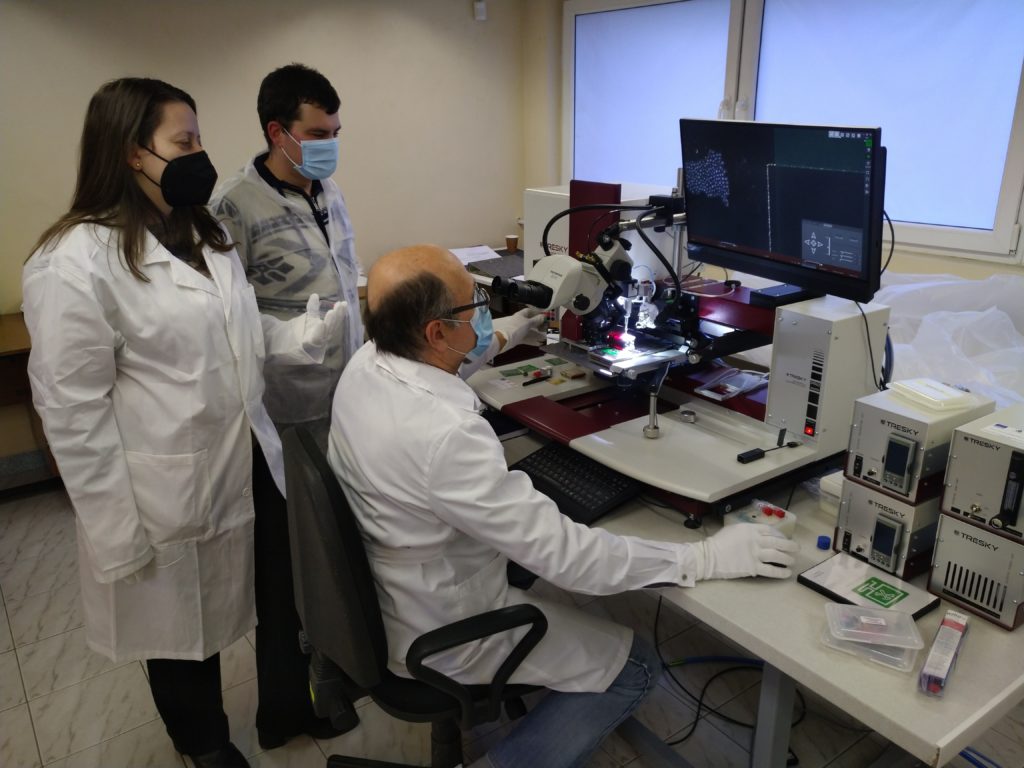
Semi-automatic die bonder
Unique specialized configuretion based on the Swiss modular complex TRESKY T-3002-PRO with the ability to move with a step of 1 µm, placement force with a step of 0.01N, working area over 100×100 mm. There is a possibility for mounting with gluing, soldering, ultrasonic and thermocompression bonding, at heating tempera-tures of the tools and table up to 400 °С and heat rate 25 °С/s. Possibility for flip chip die assembly and leadless packaging. Alignment according to X, Y, Z, Θ with calibration of 1 µm. Ability to work in an inert environment. Programmable process parameters with high repeatability, including temperature profile.
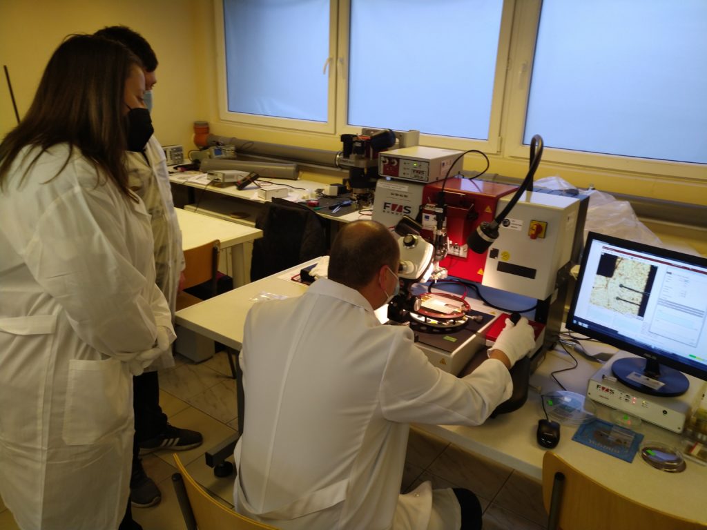
Semi-automatic wire bonder
Complex station configured for ball-wedge and wedge-wedge bonding based on universal bonder and tester model 5600 from F&S Bondtec Semiconductor GmbH, Austria.
The wiring is performed by ultrasonic bonding of gold wire with diameters from 18 to 50 µm and bonding with aluminum wire with diameters from 18 to 75 µm. Working space – 100×100 mm. Heating by programmable controller up to 250 ° C improving the reliability of the bonds.
Displacement resolution of 0.25 µm with programmable loop and possibility to multiplication of the bonds in the X / Y plane. Programmable bond loop for close, short, vertical or low conductive wire placement. Specialized software for performing three-point bonding with increased reliability (safe-bump), low bond with three-point bonding (stitch-on-ball). Bonding head for wedge-wedge bonding with 360 degrees orientation without rotation of the base.
Testing head for checking the mechanical durability of the bonds and software control of the modes.
