LABORATORY FOR THE STUDY OF NANOSTRUCTURES
PROJECT BG05M2OP001-1.001-0008 | NATIONAL CENTER OF MECHATRONICS AND CLEAN TECHNOLOGIES
Prof D.Sc. Nikolay Vitanov, Institute of Mechanics –BAS
e-mail: vitanov@imbm.bas.bg
Prof Roumen Iankov, Institute of Mechanics
e-mail: iankovr@abv.bg
tel. +359 895006340
Characterization of new materials and thin coatings by numerical experimental approach based on numerical simulation of the nanoindentation process and identification of the parameters of the material model based on nanoindentation data. A modern non-destructive approach based on nanondentation measurements and numerical methods for solving the nonlinear boundary value problem describing the nanoindentation process will be used.
ACTIVITIES
The laboratory develops material models of new bulk and layered materials and thin coatings as well as nanostructured materials.
SERVICES
- Identification of material parameters by nanoindentation.
- Numerical simulation of the nanoidentification process.
- Numerical simulation of technological processes in plastic deformation.
- Numerical simulation of processes of deformation and destruction of industrial facilities and equipment taking into account conjugate physical effects
EQUIPMENT
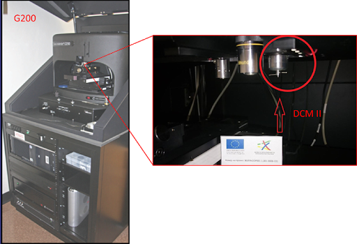
Dynamic Contact Module II (DCM II) Option of Nanoindenter G200
Тhe DCM II option of Nanoindenter G200 is a fully dynamic indentation head for ultra-low-load mechanical properties characterization. The DCM II extends the range of load-displacement experimentation down to the surface contact level.
This option extends the maximum loading capability to 30 mN and offers a full 70 μm range of indenter travel with 0.2 pm displacement resolution. Tip exchange is designed for quick removal and easy installation of a variety of application-specific tips. With the DCM II option can be studied not only the first few nanometers of indentation into the surface of a material, but also the pre-contact mechanics. Real-world testing shows that the G200 equipped with the DCM II option typically delivers noise levels less than 1 Å, supporting high resolution measurements.
The system allows dynamic nanoindentation testing of:
– Semiconductor, thin films, MEMS;
– Hard coatings, DLC films;
– Composite materials, fibers, polymers;
– Metals, ceramics, biomaterials.
