LABORATORY FOR OPTICAL AND MECHATRONIC TECHNOLOGIES
PROJECT BG05M2OP001-1.001-0008 | NATIONAL CENTER OF MECHATRONICS AND CLEAN TECHNOLOGIES
Manager: Assoc. Prof. Todor Petrov (TU – Sofia and ISSP – BAS)
e-mail: petrovts@gmail.com
tel:+359 899 361287
The laboratory is a joint scientific structure between ISSP – BAS and TU – Sofia in the frame of the project National center of mechatronics and clean technology. The laboratory staff works on the development, research and integration of laser technology systems with short and ultrashort pulses for precise processing of materials – laser micro- and nanomachining, 3D laser processing, precision laser texturing of surfaces, and others. He is interested in cooperation with science and industry partners from the country and abroad.
ACTIVITIES
The lab works mainly on:
- Development of modern laser systems with short and ultrashort pulses for laser processing of materials;
- Development, testing and optimization of laser technologies based on interaction of short and ultrashort laser pulses – laser micro- and nanomachining, laser microstructuring of surfaces, laser ablation without thermal effects, 3D laser machining, etc.;
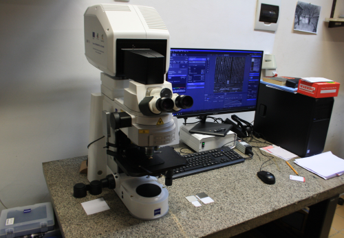
- Characterization of samples with confocal optical microscope with scanning module in a scheme with reflected light - for biomaterials and medical applications for the study of cell growth on metal surfaces and implants and other applications; for laser technologies - for monitoring the results of laser micro- and nanoprocessing and others.
SERVICES
- Development of modern laser systems with nano-, pico- and femtosecond pulses for laser machining of materials;
-
Development, testing and optimization of laser technologies for precision laser machining of materials:
-Laser micro- and nano machining – microcutting, micromilling, microengraving, drilling of microholes of/in metals, ceramics, sapphire, glass;
-Laser micro- and nano-structuring of surfaces –manufacturing of hydrophobic surfaces, change of coefficient of friction;
-3D laser processing of materials – microcutting and laser 3D engraving;
-Controlled laser ablation of thin layers;
-“Cold laser ablation” without thermal effects; -
Characterization and visualization of material surfaces with confocal laser scanning microscope:
-Characterization of surface roughness, measurement of thickness of metallographic layers, step measurement;
-Analysis of diffraction elements, topographic analysis;
-Characterization of cells growth on metal surfaces;
-Characterization of cell growth on implants surfaces;
-Modelling of corrosive layers on enamel.
EQUIPMENT
SYSTEM FOR MICRO- AND NANO-PROCESSING OF MATERIALS
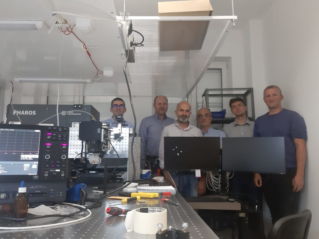
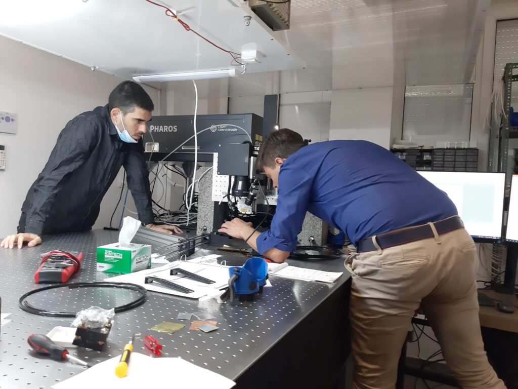
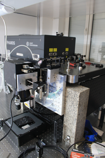
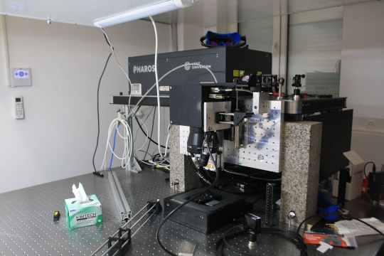
Laser Pharos PH2-SP-HP with BiBurst (LIGHT CONVERSION INC.) – due to its tunability this laser system covers a wide range of applications which normally require a few different laser sources:
- Pulse duration in the range 170 fs – 20 ps with continuous adjustment;
- Wavelength – 1030 nm, 515 nm and 353 nm;
- Repetitions frequency – single pulse to 1 MHz;
- Pulse energy up to 0.5 mJ;
- Average power 10 W;
- Polarization – linear, horizontal;
- Beam quality – TEM00; M2 < 1.3;
- Spot size – 2.9 mm;
- Module for generation of pulse packets – tunable GHz and MHz burst with burst-in-burst capability with the possibility of control of individual pulse duration and pulse to pulse delay.
Laser scanner IntelliSCAN III 14 (SCANLAB GmbH) with a f-theta lens (LINOS GmbH) with software for control laserDESK– allows precise guiding of the laser beam:
- Working field 95 mm x 95 mm (1030 nm, f = 160 mm);
- Lens coating for 353 nm, 515 nm and 1030 nm;
- Marking velocity up to 2.0 m/s
- Positioning velocity up to 5.0 m/s
- Writing speed up to 680 cps.
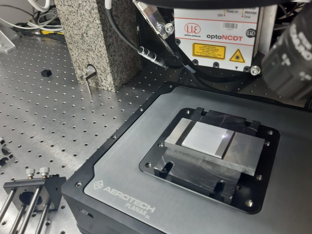
Two-axis linear positioning stage PlanarDL100XY (AEROTECH INC) and vertical linear nano-positioning stage ANT130LZS-035 (AEROTECH INC) with software for control A3200 Motion Composer and software for CADFusion for object design – for precise positioning (XYZ) of the object for processing:
- Travel XY-axes 100 mm x 100 mm;
- Accuracy XY-axes ±0.4 µm;
- Maximum velocity XY 500 mm/s;
- Travel Z-axis 35 mm;
- Accuracy Z-axis ±2.5 µm;
- Minimal incremental step Z-axis 2 nm.
Laser displacement sensor ILD2300-20 (Micro-Epsilon Inc.) – for precise control of the position of the object for processing along Z-axis:
- Measurement range 20 mm;
- Resolution 0.3 µm.
SYSTEM FOR PRECISE PROCESSING OF MATERIALS WITH SHORT LASER PULSES
The purchase of an integrated laser system with nanosecond pulses for 3D processing of materials is forthcoming – this laser system will allow the performance of a number of industrial and technological applications – laser cutting, laser engraving, laser welding, and others.
SYSTEM FOR CHARACTERIZATION OF MATERIALS
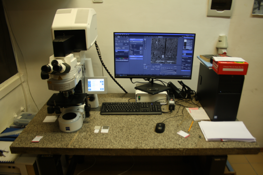
Laser scanning microscope Zeiss LSM 900 uses laser light in confocal setup with scanning module to create 3D or 2D representation of the studied sample. ZEISS LSM 900 can work in various regimes: Brightfield и Darkfield, Circular Differential Interference Contrast, Polarization Contrast и Polarization.
- Base – Axio Imager.Z2m;
- Z drive minimal displacement 10 nm;
- Laser module 405 nm single mode 5 mW;
- Scanner – two individual galvanometric scanning mirrors;
- Scanning resolution from 32 × 1 pixels till 6,144 × 6,144 pixels;
- Scanning speed – max 8 images/se with 1024 × 256 pixels
max 2 images/s with 1024 × 1024 pixels;
- Magnification during scanning 0.5× to 40×;
- Field of view during scanning – 12.7 mm × 12.7 mm;
- Lateral resolution up to 120 nm;
- Aperture – controlled diameter of the working aperture;
- Data – 8-bit and 16-bit;
- ZEN Imaging Software: software protocol for measurements – topography, layers thickness, fluorescence, microscopy;
- ConfoMap: software package for analysis and reconstruction of topographic data.
NEWS
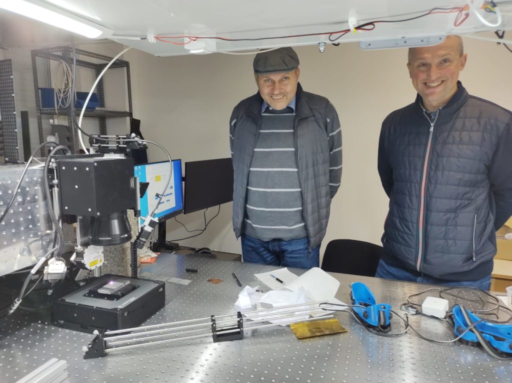
Visit to the laboratory from the group of Assoc. Prof. Marek Kocik, D.Sc, Head of the Application of Plasma and Laser Engineering Department, The Szewalski Institute of Fluid-flow machinery, Polish Academy of Sciences.
